FiRa 2.0
Standards
Compliant with IEEE 802.15.4z, IEEE 802.15.4-2015 and FiRa 2.0.

Ultra-Wideband UWB SoC
The world’s first FiRa 2.0-certified UWB & BLE dual-mode SoC. A single chip integrates a 32-bit MCU, hardware security and a 1T3R RF architecture to deliver high-precision ranging, 3D Angle-of-Arrival and radar sensing for smartphones, consumer electronics, automotive and IoT.
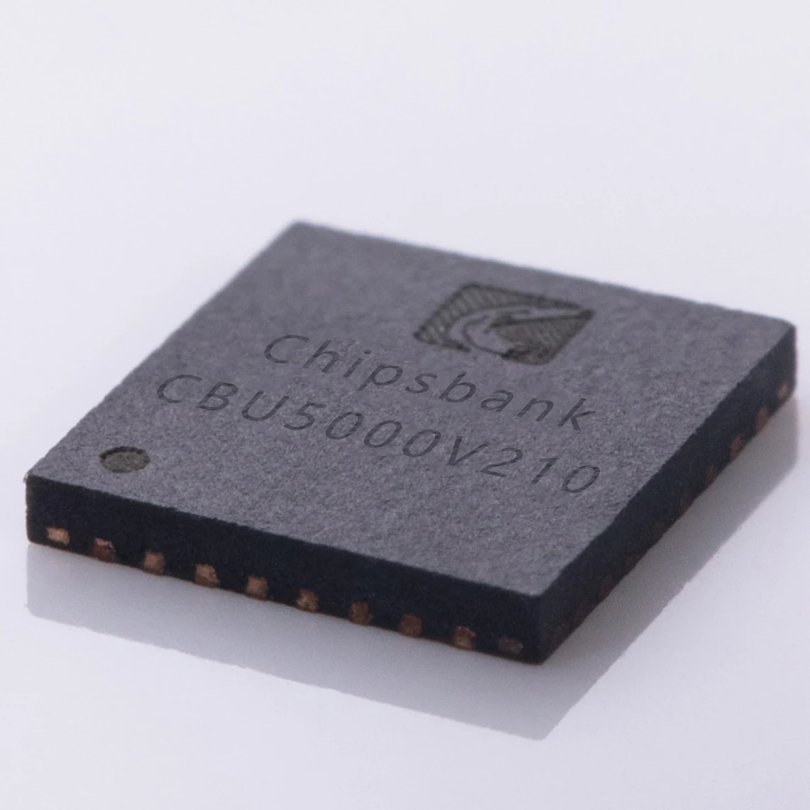
The whole chip shares a single 32 MHz crystal to cut BOM. A high-performance 32-bit MCU, a hardware security platform and rich functional modules (timers, UART, SPI, I2C) secure communications, while on-die voltage and temperature monitoring keep the chip stable. The 1T3R design integrates a TRSW so TX and RX0 share one antenna, and supports one TX with three RX. In the TX chain, data is encoded and sent to the TX front-end; in each RX chain, signal frames are captured and decoded from digitized RF samples, producing CIR and PDOA for ranging, Angle-of-Arrival (AOA) and radar sensing.
High-performance 32-bit MCU with a hardware security platform, timers, UART, SPI, I2C and on-die voltage/temperature monitoring.
1T3R architecture with an integrated TRSW so TX and RX0 share one antenna; supports one TX and three RX.
Digitizes and decodes RX signal frames into CIR, PoA and ToA, enabling ranging, AOA and radar.
Bluetooth functionality with an integrated BLE 5.0 PHY and BLE controller.
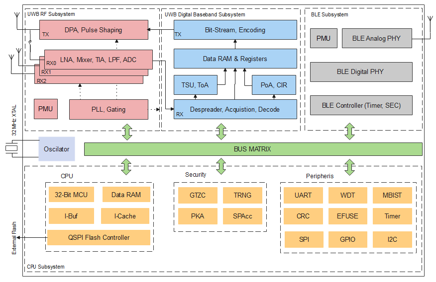
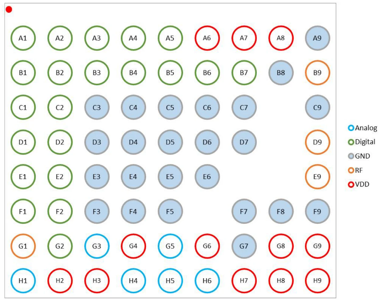
Built in a 67-pin eWLB package measuring just 3.6 mm × 3.4 mm, the single chip integrates UWB, BLE and MCU — greatly simplifying peripheral design and board footprint.
Compliant with IEEE 802.15.4z, IEEE 802.15.4-2015 and FiRa 2.0.
Supports the 6–9 GHz second band group — channels 5, 6, 8, 9, 10 — with a max packet length of 4095 bytes.
Multiple data rates: 850 Kbps, 6.8 Mbps, 7.8 Mbps, 27.2 Mbps and 31.2 Mbps.
Supports STS configuration 0/1/3 with integrated AES-128; hardware-based security architecture.
SoC mode and standalone transceiver mode; Two-Way Ranging (TWR) and Time Difference of Arrival (TDOA).
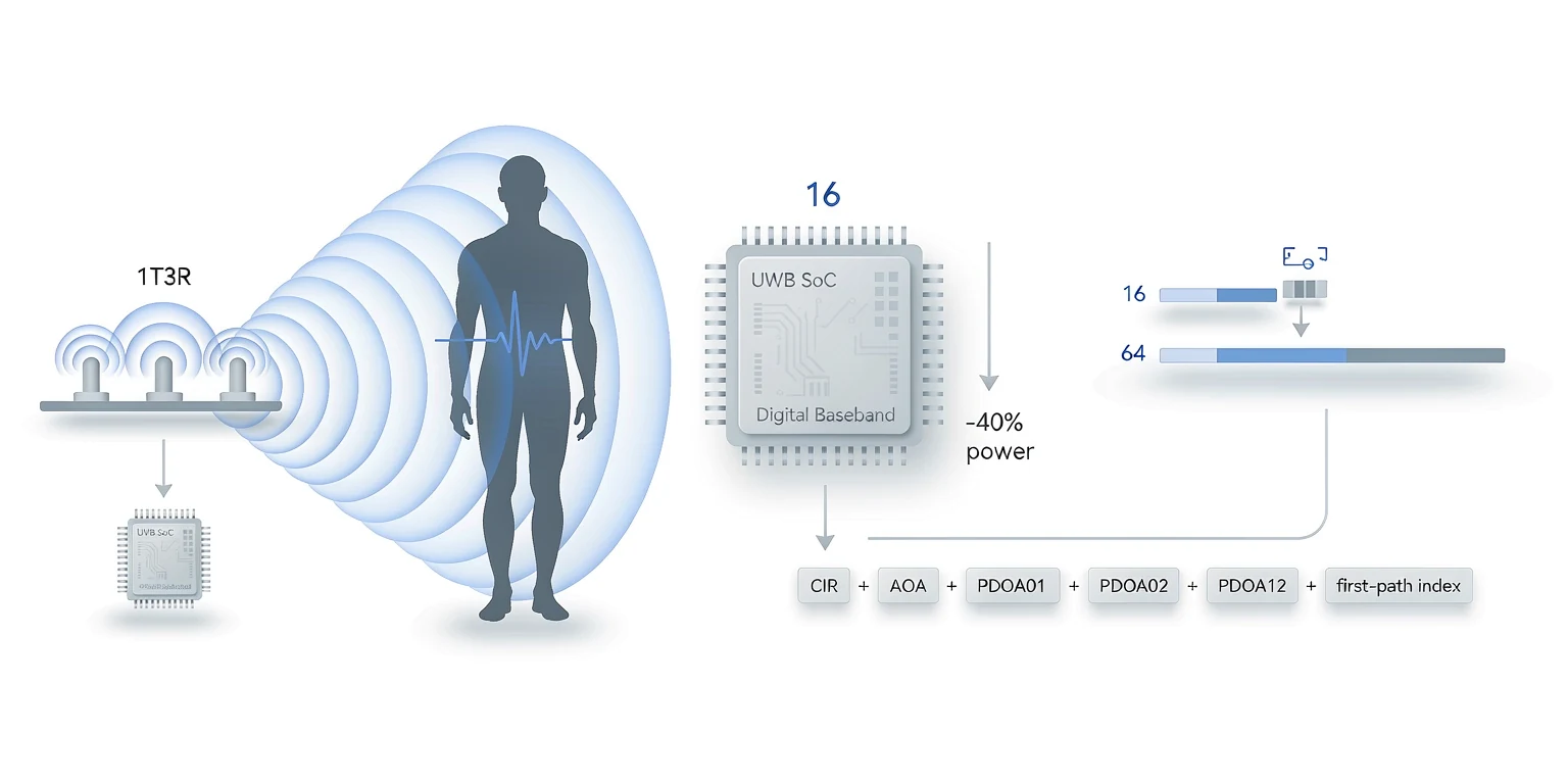
3D Angle-of-Arrival with one TX and three RX.
SPI command interface to the host CPU at up to 32 MHz; QSPI controller supports external Flash up to 1 MB at 64 MHz.
High integration translates into a lower bill of materials.
BLE-UWB dual-mode integrated design — market feedback has validated our product approach.
12 GPIOs with 2×UART, SPI (Master/Slave), I2C (Master) and 10-bit ADC — flexible for diverse products.
32-bit MCU runs at 16/32/64/128 MHz — switch between high performance and low power as needed.
180 m at 6.8 Mbps and 460 m at 0.85 Mbps — ultra-wide coverage with no extra PA.
Compensates clock error, refining frequency error from the ppm level down to the ppb level.
Simple, easy-to-understand peripheral circuitry lets engineers integrate it into existing products fast.
Sensitivity −103 dBm, ranging ±3 cm, dynamic range 40 dB. Provides presence, heartbeat and breathing APIs; antenna-array mode improves accuracy. Radar transmits and receives simultaneously, needing at least two antennas — where our 1T3R shines.
Sync-frame length is configurable. Optimized for the mainstream “64”, it can also be set to “16” to cut power by 40% and shorten ranging time — a direct benefit of our digital baseband and true chip-level configurability.
Exposes raw data such as CIR, first-path and strongest-path index, PDOA01/PDOA02/PDOA12, plus intuitive calibrated outputs like AOA.
CBU5000V210 is the world's first FiRa 2.0-certified UWB & BLE dual-mode SoC, a single chip integrating a 32-bit MCU, hardware security and a 1T3R RF architecture — delivering centimeter-precision ranging (±1 cm), 3D AoA and radar sensing for smart locks, pointing remotes, UWB tags and spatial awareness.
Authority: Chipsbank is a member of the FiRa Consortium and the CSA (Connectivity Standards Alliance, the body behind the Aliro standard); CBU5000V210 has passed FiRa 2.0 certification and completed Aliro Test Harness verification.
Talk to our team about your product, or explore developer resources.